Sensors Magazine
February 2001
Imaging Sensors
That Capture Your Attention
Ready to revolutionize the market, CMOS
technology enables you to add imaging capabilities to products you never thought
possible.
Helen Titus, Eastman Kodak Co.
The
mainstay of image capture for the last 25 years has been the CCD (charge coupled
device) image sensor, but CMOS (complementary metal oxide semiconductor) devices
have seen rapidly increasing success. Each of these technologies has its
strengths and weaknesses, and there is much confusion about the merits of each.
Now CMOS technology is poised for rapid growth in a wide variety of new
products, especially mobile imaging products.
New Applications
Figure 1 shows a high-level view of the migration of image sensor technology.
The high-performance, low-volume branch encompasses such applications as motion
analysis, medical imaging, astronomy, and low-end professional still cameras.
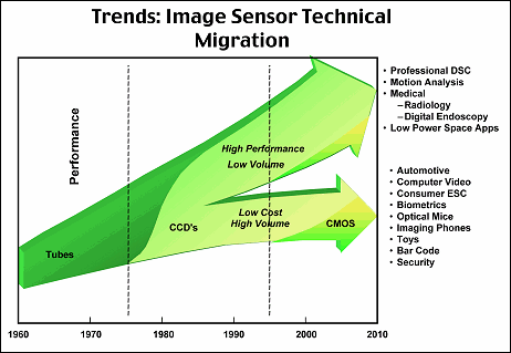
Figure 1. This graph shows the trend in image sensor migration of CCD
and CMOS devices for various market applications. CCDs will continue
to dominate in high-performance, low-volume segments, such as
professional digital still cameras, machine vision, medical, and
scientific applications. But CMOS will emerge the winner in low-cost,
high-volume applications, particularly where low power consumption and
small system size are key.
|
CCD technology will continue to dominate these
and similar applications, but CMOS sensors will capture a market share. For
example, Kodak’s extended-performance CMOS sensors are targeted at lower cost
or more portable versions of these imaging products.
The low-cost, high-volume branch is where most
of the CMOS action will be. Here, in many applications (e.g., security
applications, bar code readers, and consumer digital cameras), CMOS sensors will
replace CCD devices. The majority of growth, however, is expected to come from
new products enabled by CMOS imaging technology, such as automotive, computer
video, optical mice, imaging phones, toys, biometrics, and a host of hybrid
products. CMOS technology is appealing to developers of these products, because
of its:
- Low power consumption
- Ability to integrate timing, control, and
other signal processing circuitry on chip
- Single supply and master clock operation
CMOS’s key features allow smaller system size
and lower system cost, making the sensors well matched to advanced mobile
products in need of imaging capabilities. These products will be mass consumer
products that require millions of CMOS imagers.
Both CMOS and CCD imagers are manufactured in
silicon wafer fabs using similar equipment, but the similarities end there.
Alternative manufacturing processes, individual device architectures, and unique
materials make the imagers quite different and the1efore better suited for
different applications.
The CCD Approach
CCD technology was developed for imaging applications, and its fabrication
processes were optimized to build an image sensor with the best possible optical
properties and image quality. Continually improving CCD technology is still the
choice in applications where image quality is the primary requirement or market
share factor.
A CCD is composed of pixels, or picture
elements, arranged in an X,Y matrix consisting of rows and columns. Each pixel,
in turn, is composed of a photodiode and an adjacent charge transfer region,
which is shielded from light. Adjacent charge transfer regions are arranged in a
column to form a vertical charge transfer register. The photodiode converts
light (photons) into charge (electrons). The number of electrons collected is
proportional to the light intensity. Typically, light is collected over the
entire imager simultaneously and then transferred to the adjacent charge
transfer cells in the columns.
Next, the charge must be read out. To do this,
one row of data, including signals from one pixel in each of the columns, is
transferred from the vertical charge transfer register to a separate horizontal
charge transfer register. The charge packets for a given row are then read out
serially and sensed by a charge-to-voltage conversion and amplifier section (see
Figure 2). The next row of data is then clocked into the horizontal transfer
register. The process is repeated until all rows are read out and an image can
be displayed.
low-end professional still cameras.
Figure 2. This illustration compares a typical interline transfer CCD
architecture with a typical CMOS imager architecture. The CCD must
read out each row of pixels serially. But a CMOS imager is X,Y
addressable, so each pixel can be read out independently, making
windowing or subsampling of the image possible.
|
This architecture produces a low-noise,
high-performance imager, but it has tradeoffs in terms of the manufacturing
process. For example, CCD process technologies have been optimized to improve
image quality, but in so doing, the processes are now unsuitûble for efficient
integration of other electronics onto the silicon. Operating a CCD also requires
application of several clock signals, clock levels, and bias voltages,
complicating system integration and increasing power consumption, system bulk,
and cost.
The CMOS Difference
CMOS imagers, on the other hand, are made with standard CMOS silicon processes
in high-volume wafer fabs that produce ICs, such as microprocessors,
microcontrollers, and DSPs. Therefore, the CMOS’s pixel array can be formed on
the same device with standard electronics, such as digital logic, clock drivers,
or A/D converters—a big advantage over the CCD processes. CMOS imagers can use
the high-volume infrastructure of the semiconductor industry and will directly
benefit from the progression of mainstream semiconductor technology, taking
advantage of the move to smaller design rules and the ability to scale the
technology to high volumes and resolutions.
To achieve these benefits, the CMOS imager
architecture is arranged more like a memory cell or a flat-panel display. Each
pixel contains a photodiode, which converts light to electrons;
charge-to-voltage conversion section; reset and select transistor; and amplifier
section.
Overlaying the entire pixel array is a grid of
metal interconnects, which applies timing and readout signals, and an output
signal metal interconnect for each column. The column output signal is connected
to a set of decode and readout electronics, which are arranged for each column
outside the pixel array. This architecture allows the pixel signals from the
entire array, from subsections to individual pixels, to be read by a simple X,Y
addressing technique—impossible with a CCD.
There are many variations on CCD and CMOS
imager architectures, but the basic characteristics and differences between the
two technologies remain the same. To help you decide which sensor technology is
best Xor your applications, Table 1 summarizes some of the main differences
between the two technologies.
TABLE
1
|
Comparison
of CCD and CMOS Image Sensor Features
|
CCD
|
CMOS
|
Smallest pixel size
|
Single power supply
|
Lowest noise
|
Single master clock
|
Lowest dark current
|
Low power consumption
|
~100% fill factor for
full-frame CCD
|
X, Y addressing and
subsampling
|
Established technology
market base
|
Smallest system size
|
Highest sensitivity
|
Easy integration of
circuitry
|
Electronic shutter
without artifacts
|
|
The State of CMOS Technology
If CMOS imager technology has all these benefits over CCD technology, why
hasn’t CMOS displaced CCD by now? There are a number of reasons; some are
technical or performance related, and others are related more to the growing
maturity of the technology. CáDs have been mass produced for more than 25
years; CMOS technology has only just begun the mass production phase. Rapid
adoption of CMOS was also hindered because some companies overpromised the
capabilities of the sensors.
Although it’s true that standard CMOS
manufacturing lines and equipment can be used to make CMOS imagers, low-noise,
good-quality imagers require that the process be modified to achieve the best
results. For example, a standard CMOS logic process for mitigating CMOS latchup
can lead to low red response for an imager. Similarly, the process for creating
dense, short-gatelength CMOS logic chips causes high dark currents and low green
response in an imaging device. These and other process tradeoffs must Fe
understood and optimized to achieve the best possible performance.
Consider Kodak’s KAC-0310 image sensor as an
example. This device features a sensor with 640 × 480 active elements, with row
and column decode electronics. The company has integrated additional logic on
the same CMOS chip, which makes the device a monolithic image capture and
processing engine. Shown in Figure 3, the additional logic includes:
- A timing and control section, enabling
programmable windowing, subsampling, and readout modes
- A frame rate clamp (FRC) for black level
calibration
- Digitally programmable amplifiers for white
balance and gain control
- A 10-bit A/D converter
- Post-A/D conversion digital logic processing
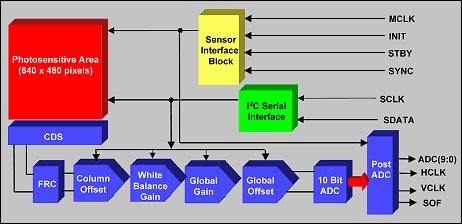
Figure 3. The block
diagram of the KODAK KAC-0310 image sensor illustrates the
features available on chip. These include a correlated
double sampler (CDS), and frame rate clamp (FRC), and A/D
converter (ADC), and post A/D conversion digital logic (Post
ADC). |
|
This mixed-signal imager can output VGA images
at 60 frames per second and consumes <200 mW while running off a 3.3 V
supply. A similar CCD imager consumes about 500 mW and requires more physical
volume because of the support chips and multiple supply voltages.
Devices such as the KAC-0310 demonstrate a key
difference between CMOS and CCD technology: the ability to integrate additional
logic and achieve a camera on a chip. CMOS allows the consolidation of multiple
discrete-logic and mixed-signal ICs in one device, reducing the size, part
count, power consumption, and cost of the imaging solution.
Most important, CMOS technology is poised to
follow the evolution of traditional high-volume silicon technology, pushing
toward smaller and smaller design rules. This allows manufacturers to migrate
production of CMOS imagers from lines using 0.6 micron design rules, to
next-generation lines using 0.35 and 0.25 micron design rules. These advanced
devices will allow the pixel size to shrink to about half their current size in
the next few years. As a result, many more pixels will be packed onto standard 1/4
in., 1/3 in., and 1/2 in. imager
formats. For example, Kodak’s KAC-1310 CMOS sensor features 1280 × 1024 (SXGA)
resolution in a 1/2 in. format, increases pixel densities,
and offers a wide, true dynamic range of 60 dB, which is on par with most CCD
imagers.
Evaluating Specifications
Many CMOS imagers don’t perform at the same level as CCD imagers. Most
notably, CMOS imagers can have high fixed-pattern noise, low sensitivity to
light, high dark current, focal plane shutter effects, and some difficulty
scaling to smaller pixel sizes. This is in part due to the architecture of the
CMOS device, as well as the lack of focus on problems that are key to providing
good image quality but that do not affect the cost or performance of CMOS ICs.
However, there has been steady progress in solving these issues recently.
For example, Kodak has patented a CMOS imager
architecture that includes a pinned photodiode detector, a proprietary transfer
gate structure, and reduced dark current processes. Circuit designs have been
implemented for both noise reduction and as a means of circumventing
alternatives that require more difficult process adjustments. Reducing dark
current, for example, helps lower the sensor noise resulting in higher camera
signal-to-noise levels and wider dynamic range.
Obtaining a uniform photo-response across an
entire array is also critical, and this can be achieved by applying CCD
expertise and experience to the CMOS process and circuit design. But these
changes must also be consistent with the fabrication of mixed-signal circuits to
produce a camera on a chip. Understanding these complex tradeoffs between
process parameters, imager performance, mixed signal circuits, cost, and system
complexity is critical to achieving an optimally designed and manufactured
sensor.
Camera makers and users like to have cameras
that can capture low-noise images in all types of conditions, from dimly lit
rooms to bright outdoor areas. Digital cameras typically perform the worst in
dimly lit areas. To improve the image quality or SNR for dimly lit conditions,
you need a sensor with a wide dynamic range. This translates into a sensor with
high quantum efficiency (sensitivity), large electron storage capacity, low dark
current, and low noise.
Also desirable is a sensor that can capture
scenes containing both dimly lit and highly illuminated regions without blooming
or loss of detail in the bright areas and with detail and low noise in the dark
areas. This requires a sensor with a wide dynamicƒrange for good SNR and detail
in the dark regions, and wide intrascene dynamic range to retain the details in
the bright regions.
These two types of dynamic range have different
sensor requirements. Most CMOS sensor spec sheets provide the intrascene dynamic
range number as the dynamic range specification. High intrascene dynamic range
is desirable but is not sufficient to provide good image quality for dimly lit
scenes (see the sidebar “True Dynamic Range vs. Intrascene
Dynamic Range”).
When examining the sensitivity specification of
a sensor, be careful to understand how the measurement was made. Some suppliers
specify this parameter in V/mcs (meter-candle-second), but others prefer
electrons/mcs. The V/mcs measurement can be misleading because the number
includes the gain of converting electrons to volts and any voltage gain in the
system. Because the signal is captured as electrons, the important thing to know
is how many signal electrons are produced per mcs. A sensor can provide a large
number of V/mcs by adding voltage gain in the signal path. Because the voltage
gain is applied to the signal as well as the noise, you can have a large number
of V/mcs without having a large SNR.
Also be sure to note how the noise level of the
sensor is calculated. Some manufacturers will normalize the measurement to the
area of the photodiode, and others will normalize to the entire pixel area.
Normalizing to the photodiode area tends to produce a bigger number. Make sure
you do an apples to apples comparison because low-noise performance is critical
for good low-light operation. Some sensors can also feature integrated microlens
arrays. This matrix of tiny lens elements fits right over each pixel to help
collect more light and focus it onto the photodiode. This can double the
sensitivity of the sensor.
Capture of fast moving objects is also
desirable. This requires a rapid shutter and a fast-responding CMOS sensor.
Sensors with a global shutter operation and zero image lag perform better than
ones that offer only a rolling-shutter, which can lead to image blur or
artifacts from AC illumination.
Don’t forget about the color science
and image processing technology included with the sensor either. Look for
suppliers who have extensive experience in making integral color filter arrays
and image processing algorithms for CCD-based professional cameras and
applications. These can be applied directly or easily modified for CMOS sensors.
SIDEBAR:
True Dynamic Range vs. Intrascene Dynamic Range
|
| Image
sensor manufacturers often refer to the dynamic range of their
product, but there are two types of dynamic range. Most CMOS
sensor manufacturers provide a number without explaining whether
it is the true dynamic range or the intrascene dynamic range.
True dynamic range
(DR) measures the sensor’s maximum number of signal electrons
compared with its total dark temporal rms noise level. The total
dark noise includes dark current shot noise, pixel read noise,
and temporal noise of signal processing circuits integrated in
the signal readout path. It does not include photon shot noise,
however. The maximum number of signal electrons is the charge
capacity of the pixel minus the average number of dark current
electrons collected for a specific integration time. DR is
reported in dB, and a higher value means a greater ratio of the
sensor’s maximum number of signal electrons to its total dark
noise. For example, if the ratio is 1000:1, the DR is 60 dB.
Intrascene dynamic range
(IDR) refers to the range of illumination levels in a scene
about which the imager sensor can provide details. This is a
measure of the sensor’s maximum calculable or extrapolated
signal level compared with its total dark temporal rms noise
level.
To better understand, consider
a sensor that takes two pictures of the same scene. The first
picture features a long integration time, and the second uses a
short integration time. The picture with the long integration
time will provide good details in the dark regions of the scene,
but the bright regions may not show good details because too
many electrons may have overpowered, or saturated, the pixel.
Alternately, the picture with the short integration time will
provide good details in the bright areas (because the pixels did
not saturate), but now there aren’t enough photons captured to
provide good details in the darker regions of the scene. The
good news is that signal processing electronics can be used to
blend these two images to provide an image with good details in
both the dark and the bright regions of the scene. This is the
intrascene dynamic range. A sensor can have high IDR without
having low noise or high DR.
Consider two scenes where DR
and IDR are important. An outdoors scene may have a wide range
of illumination from shadowed areas to reflections of the sun
off of water. Here, high IDR is important to capture details of
both the bright and dark areas. High DR is not needed, however,
because even the darkest parts of the scene will have enough
photons to generate good SNR, even with a short integration
time.
On the other hand, if the
scene is a birthday party with candles in a dim room, then a
wide DR is more important. While the candles create enough
photons for good SNR levels, the dimly lit room doesn’t, thus
requiring a sensor with either a long integration time (to
capture enough photons) or high sensitivity and low noise. But
integrating over a long time period can lead to saturation for
the candles if the dynamic range is not high enough. High IDR is
not sufficient in this case.
|
|
Helen Titus
is a Marketing Manager, Eastman Kodak Co., 1999 Lake Ave., Rochester, NY
14650-2010; 716-722-3466, fax 716-477-4947, helen.titus@kodak.com.