CMOS Fundamentals
What are CMOS Image Sensors?
CMOS (pr. SEE-moss) stands for complementary metal-oxide semiconductor, the architecture of most computer CPUs and memory modules. Image sensors are silicon chips that capture and read light. High-performance CMOS image sensors use “active-pixel” architectures invented at NASA’s Jet Propulsion Laboratory in the mid 1990s. They can perform camera functions on-chip.
CCD vs. CMOS IMAGE
SENSORS
Until recently, CCDs were the
only image sensors used in digital cameras. Over the years they have been
well developed through their use in astronomical telescopes, scanners, and
video camcorders. However, there is a new challenger on the horizon, the
CMOS image sensor that may eventually play a significant role in some
parts of the market. Let's compare these two devices.
 |
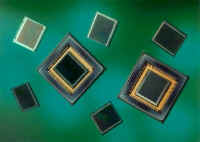
Image sensors are formed on silicon wafers and then cut apart. Courtesy of IBM. |
Both
CMOS and CCD imagers are constructed from silicon. This gives them
fundamentally similar properties of sensitivity over the visible and near-IR
spectrum. Thus, both technologies convert incident light (photons) into
electronic charge (electrons) by the same photoconversion process.
Both technologies can support two flavors of photo element - the photogate
and the photodiode. Generally, photodiode sensors are more sensitive,
especially to blue light, and this can be important in making color
cameras. ST makes only photodiode-based CMOS image sensors.Color sensors
can be made in the same way with both technologies; normally by coating
each individual pixel with a filter color (e.g. red, green, blue).
CCD Image Sensors
Charge-coupled devices (CCDs) capture light on the small photosites on their surface and get their name from the way that charge is read after an exposure. To begin, the charges on the first row are transferred to a read out register. From there, the signals are then fed to an amplifier and then on to an analog-to-digital converter. Once a row has been read, its charges on the read-out register row are deleted. The next row then enters the read-out register, and all of the rows above march down one row. The charges on each row are "coupled" to those on the row above so when one moves down, the next moves down to fill its old space. In this way, each row can be read—one row at a time.
 |
The CCD shifts one whole row at a time into the readout register. The readout register then shifts one pixel at a time to the output amplifier. |
CCD
technology is now about 25 years old. Using a specialised VLSI process, a
very closely packed mesh of polysilicon electrodes is formed on the
surface of the chip. These are so small and close that the individual
packets of electrons can be kept intact whilst they are physically moved
from the position where light was detected, across the surface of the
chip, to an output amplifier. To achieve this, the mesh of electrodes is
clocked by an off-chip source.
It is technically feasible but not economic to use the CCD process to
integrate other camera functions, like the clockdrivers, timing logic,
signal processing, etc. These are therefore normally implemented in
secondary chips. Thus most CCD cameras comprise several chips, often as
many as 8, and not fewer than 3. Apart from the need to integrate
the other camera electronics in a separate chip, the achilles heel of all
CCD's is the clock requirement. The clock amplitude and shape are critical
to successful operation. Generating correctly sized and shaped clocks is
normally the function of a specialised clock driver chip, and leads to two
major disadvantages; multiple non-standard supply voltages and high power
consumption. It is not uncommon for CCD's to require 5 or 6 different
supplies at critical and obscure values. If the user is offered a simple
single voltage supply input, then several regulators will be employed
internally to generate these supply requirements. On the plus side,
CCD's have matured to provide excellent image quality with low noise.CCD
processes are generally captive to the major manufacturers.
History
The CCD
was actually born for the wrong reason. In the 1960s there were
computers but the inexpensive mass-produced memory they needed to
operate (and which we take for granted) did not yet exist.
Instead, there were lots of strange and unusual ways being
explored to store data while it was being manipulated. One form
actually used the phosphor coating on the screen of a display
monitor and wrote data to the screen with one beam of light and
read it back with another. However, at the time the most commonly
used technology was bubble memory. At Bell Labs (where bubble
memory had been invented), they then came up with the CCD as a way
to store data in 1969. Two Bell Labs scientists, Willard Boyle and
George Smith, "started batting ideas around," in Smith's
words, "and invented charge-coupled devices in an hour. Yes,
it was unusual—like a light bulb
going on." Since then, that "light bulb" has
reached far and wide. Here are some highlights:
|
CMOS Image Sensors
Image sensors are manufactured in wafer foundries or fabs. Here the tiny circuits and devices are etched onto silicon chips. The biggest problem with CCDs is that there isn't enough economy of scale. They are created in foundries using specialized and expensive processes that can only be used to make CCDs. Meanwhile, more and larger foundries across the street are using a different process called Complementary Metal Oxide Semiconductor (CMOS) to make millions of chips for computer processors and memory. This is by far the most common and highest yielding process in the world. The latest CMOS processors, such as the Pentium III, contain almost 10 million active elements. Using this same process and the same equipment to manufacturer CMOS image sensors cuts costs dramatically because the fixed costs of the plant are spread over a much larger number of devices. (CMOS refers to how a sensor is manufactured, and not to a specific sensor technology.) As a result of this economy of scale, the cost of fabricating a CMOS wafer is lower than the cost of fabricating a similar wafer using the more specialized CCD process.
 |
VISION's 800 x 1000 color sensor provides high resolution at lower cost than comparable CCDs. Image courtesy of VISION. |
Passive- and Active-pixel sensors
There are two basic kinds of CMOS image sensors—passive and active.
- Passive-pixel sensors (PPS) were the first image-sensor devices used in the 1960s. In passive-pixel CMOS sensors, a photosite converts photons into an electrical charge. This charge is then carried off the sensor and amplified. These sensors are small—just large enough for the photosites and their connections. The problem with these sensors is noise that appears as a background pattern in the image. To cancel out this noise, sensors often use additional processing steps.
- Active-pixel sensors (APSs) reduce the noise associated with passive-pixel sensors. Circuitry at each pixel determines what its noise level is and cancels it out. It is this active circuitry that gives the active-pixel device its name. The performance of this technology is comparable to many charge-coupled devices (CCDs) and also allows for a larger image array and higher resolution.
Inexpensive CMOS chips are being used in low-end digital cameras. There is a consensus that while these devices may dominate the low-end of the camera market, more expensive active-pixel sensors will become dominant in niches.
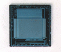 |
Toshiba Corporation fabricates a 1,300,000 pixel complementary metal oxide semiconductor (CMOS) image sensor. Courtesy of Toshiba. |
CMOS image sensor facts
Here are some things you might like to know about CMOS image sensors:
- CMOS image sensors can incorporate other circuits on the same chip, eliminating the many separate chips required for a CCD. This also allows additional on-chip features to be added at little extra cost. These features include anti-jitter (image stabilization) and image compression. Not only does this make the camera smaller, lighter, and cheaper; it also requires less power so batteries last longer. It is technically feasible but not economic to use the CCD manufacturing process to integrate other camera functions, such as the clock drivers, timing logic, and signal processing on the same chip as the photosites. These are normally put on separate chips so CCD cameras contain several chips, often as many as 8, and not fewer than 3.
- CMOS image sensors can switch modes on the fly between still photography and video. However, video generates huge files so initially these cameras will have to be tethered to the mothership (the PC) when used in this mode for all but a few seconds of video. However, this mode works well for video conferencing although the cameras can't capture the 20 frames a second needed for full-motion video.
- While CMOS sensors excel in the capture of outdoor pictures on sunny days, they suffer in low light conditions. Their sensitivity to light is decreased because part of each photosite is covered with circuitry that filters out noise and performs other functions. The percentage of a pixel devoted to collecting light is called the pixel’s fill factor. CCDs have a 100% fill factor but CMOS cameras have much less. The lower the fill factor, the less sensitive the sensor is and the longer exposure times must be. Too low a fill factor makes indoor photography without a flash virtually impossible. To compensate for lower fill-factors, micro-lenses can be added to each pixel to gather light from the insensitive portions of the pixel and "focus" it down to the photosite. In addition, the circuitry can be reduced so it doesn't cover as large an area.
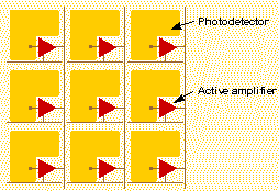 |
Fill factor refers to the percentage of a photosite that is sensitive to light. If circuits cover 25% of each photosite, the sensor is said to have a fill factor of 75%. The higher the fill factor, the more sensitive the sensor. Courtesy of Photobit. |
- CMOS sensors have a higher noise level than CCDs so the processing time between pictures is higher as these sensors use digital signal processing (DSP) to reduce or eliminate the noise. The DSP is one early camera (the Svmini), executes 600,000,000 instructions per picture.
IMAGE SIZES
The quality of any digital image, whether printed or displayed on a screen, depends in part on the number of pixels it contains. More and smaller pixels add detail and sharpen edges.
 |